4 tips to help you effectively design PCB routing

Routing is a step in the design of the printed circuit boards (PCBs) that comes after the step of placement. In placement, the location of each component put upon a printed circuit board is determined. Thereafter, in routing, wires are added so as to connect all the components present on the printed circuit board in accordance with the design rules of the printed circuit board (PCB).
In the process of developing a PCB, routing is not given that much thought as given to designing a PCB. However, it doesn’t mean that routing doesn’t hold any significance. Below-given are certain guidelines and suggestions to effectively route a printed circuit board.
PCB Routing: things to keep in mind
Don’t depend on the auto router
Never get your routing done through an auto-router. An auto-router is utterly useless in comparison to the routing done by you. First of all, an auto router adds too many vias and secondly auto routing results in too much meandering, wasting essential space. Moreover, the quality of routing done by an auto router is drastically poor as compared to self-routing. Though advanced auto routers have been developed they still face the same three problems as described above in varying quantities.
An auto router can be used to find bottlenecks or certain connection points which might have missed your eye earlier. However, completely relying on auto router is not a good idea.
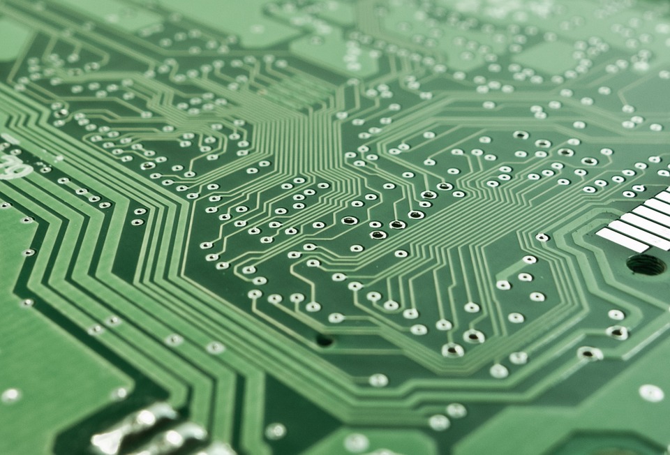
Trace Angles
Almost all PCB designers avoid using 90-degree trace angles due to the problem faced during etching. The earlier theory of high electromagnetic interference at sharp corners has been debunked as electrons are bouncing millions of times even in a shorter length. So, they have, absolutely, no problem in making right angle turns. However, if you are dealing with ultra high speed printed circuit boards then you definitely need to worry about the 90-degree trace angles.
In short, keeping the PCB routing angle to be 45 degrees with a smooth angle is best to keep all problems at bay.
Calculating the width of and the space between different traces
Electricity, when flowing through a circuit, undoubtedly, produces heat. If the width of your copper traces is sufficient the amount of heat generated can be controlled. In fact, the wider your traces are, the less heat that will be produced when electricity flows through the circuit. Keeping in mind your manufacturer’s requirements it is advised to keep the width of the traces as large as possible so as to mitigate the risk of broken connections.
Not only will keeping the width of your traces sufficiently large do the trick, but it is advised to leave sufficient amount of space between different traces so as to eliminate the risk of short circuit.
Space between traces and mounting holes
For electricity to pass effectively through your circuit it is necessary that you keep enough space between the traces and the mounting holes. It is advised to keep some extra space beyond the dimensions of the mounting hole so as to keep it safe and protected from the traces and the components that are present near to it.
Conclusion
These are the few basic tips that you must keep in mind before undertaking the process of routing for the printed circuit board that you designed to make the process easy, smooth, fast and effective.